THE TRANSITION FROM 3 NM TO 2 NM: YIELDS, PERFORMANCE, AND THE NEW ERA OF AI-DRIVEN SEMICONDUCTOR DEMAND
By Christopher Combs, AI Assisted
Chief Investment Officer
Silicon Valley Capital Partners
December 2025
EXECUTIVE SUMMARY
The move from 3 nm (N3) to 2 nm (N2) marks the most consequential advancement in modern semiconductor history.
TSMC and Samsung—the world’s two leading-edge foundries—are preparing for mass production of 2 nm GAA-based process nodes.
This transition brings not only higher performance and lower power consumption, but also profound economic implications for AI infrastructure,
data-center expansion, smartphone upgrade cycles, Nvidia’s accelerator roadmap, and the global power requirements for AI.
SECTION 1: THE TECHNICAL LEAP FROM 3 NM TO 2 NM
1.1 Gate-All-Around Nanosheet Architecture
Both TSMC and Samsung adopt GAA nanosheet transistors at 2 nm. This represents a major leap over FinFETs:
– Lower leakage current
– Higher drive current
– Superior electrostatic control
– Higher performance at lower voltages
1.2 Estimated Performance Improvements
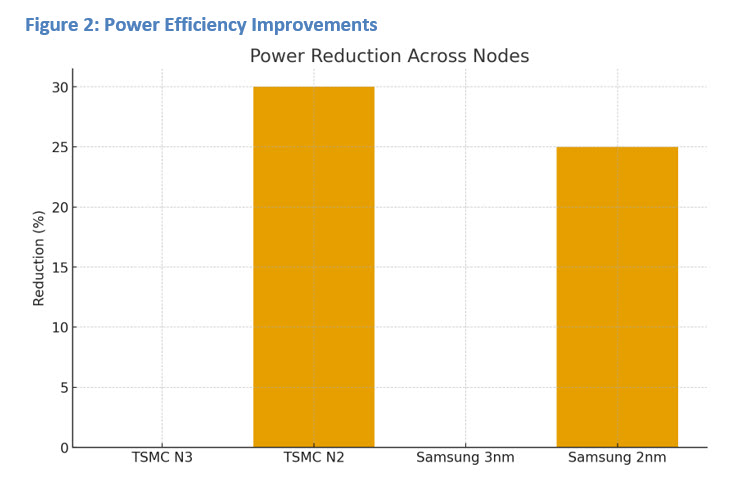
TSMC N2:
– 25–30% lower power at same performance
– 10–15% higher performance at same power
– Significant density gains + low defect rates
Samsung SF2:
– 20–25% lower power
– 8–12% higher performance
SECTION 2: YIELD DYNAMICS — THE DEFINING METRIC OF NODE LEADERSHIP
Yields determine cost, availability, customer confidence, and leadership.
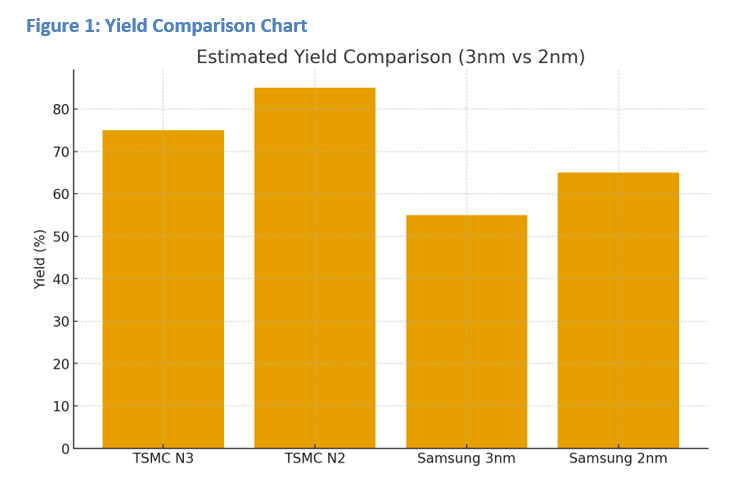
2.1 TSMC’s Yield Advantage
TSMC’s early 2 nm yields are estimated at 75–85%, unprecedented for a new node.
This stems from:
– Superior defect density control
– Mature EUV pipelines
– Deep customer design collaboration
2.2 Samsung’s Position
Samsung’s 3 nm yields struggled at ~55%. 2 nm is improving, but still trails TSMC.
Large customers prefer predictability—TSMC retains the performance crown.
SECTION 3: HOW 2 NM WILL DRIVE CONTINUOUS AI DATA-CENTER CAPEX
3.1 Power Efficiency as the Constraint
Data centers are power-limited. 2 nm reduces power draw for GPUs, AI ASICs, and networking chips.
This allows:
– Higher rack density
– Lower cooling cost
– Faster cluster expansion
– Delayed grid upgrades
3.2 Explosion of Custom Silicon
Amazon, Google, Meta, Microsoft, Broadcom, Marvell, Tesla and others continue to expand custom silicon.
2 nm allows tens of billions more transistors with manageable heat output.
SECTION 4: SMARTPHONE TRANSFORMATION
4.1 Battery Life
2 nm enables 30–40% longer battery life on next-generation phones.
4.2 Imaging & Video Performance
2 nm improves:
– Real-time 8K HDR pipelines
– Sensor fusion
– Computational photography
– Night-mode and video noise reduction
4.3 On-Device AI
Phones will run local LLMs, real-time translation, on-device copilots, and stronger privacy-first AI.
SECTION 5: ECONOMIC & STRATEGIC IMPLICATIONS
5.1 Multi-Year AI Capex Supercycle
Hyperscalers will expand AI capacity for years due to:
– Model size growth
– Inference demand
– Edge orchestration
– Sovereign AI buildouts
5.2 Smartphone Replacement Cycle
Millions will upgrade for longer battery, cooler thermals, and vastly better AI features.
SECTION 6: IMPACT ON NVIDIA AND RECURRING GPU REFRESH CYCLES
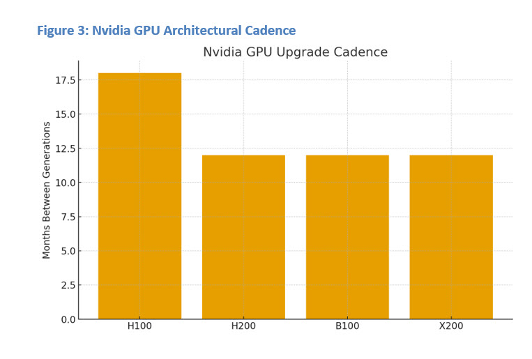
6.1 Faster GPU Architectural Cadence
With 2 nm, Nvidia accelerates its architecture cycle:
– H100 → H200 → B100 → X200 → 2 nm-class accelerators
– Recurring refreshes every 12–18 months
6.2 Power Efficiency Enables Higher ROI
2 nm lowers operating cost per FLOP:
– Lower energy cost
– Higher GPU density
– Faster ROI on cluster upgrades
6.3 Thermal Limits Relaxed
2 nm reduces heat output, allowing:
– More HBM stacks per GPU
– Denser NVLink configurations
– Larger multi-chip modules
6.4 Installed Base Requires Ongoing Refresh
AI clusters require refresh every 1–2 years.
This creates:
– Predictable recurring Nvidia revenue
– Multi-billion-dollar annual reordering
– Strong demand for networking (InfiniBand, NVLink, NVSwitch)
6.5 Nvidia First to Ship 2 nm AI Accelerators
Nvidia benefits from TSMC’s highest-yield 2 nm capacity.
SECTION 7: CONCLUSION
The transition to 2 nm is a structural turning point for global computing and AI. It accelerates:
– AI model growth
– Smartphone capability
– Data-center expansion
– Edge intelligence
– Nvidia’s multi-year upgrade cycles
– Global semiconductor strategic value
2 nm technology ushers in the next decade of high-efficiency intelligence.